
Cross-Industry Traceability: Custom Laser Marking Solutions
In the highly automated industrial ecosystem of 2026, cross-industry supply chains demand unprecedented data transparency and item-level traceability. Surface-level markings that easily smudge, peel, or corrode under operating duress are no longer just an operational inconvenience they represent immediate regulatory compliance failures and severe financial liabilities. Whether your facility is processing mission-critical flight hardware, microscopic circuit pathways, or sterile surgical instruments, structural part identification must endure the entire lifecycle of the asset.
Operating from our advanced contract processing center in Mississauga, we specialize in custom Laser Marking Solutions mathematically optimized for specific industry regulations, component dimensions, and material thresholds. By bridging cutting-edge optical systems with rigorous quality control, we translate physical parts into secure digital assets for the Greater Toronto Area’s (GTA) top engineering brands.
Precision Marking Solutions for Every Industry
INDUSTRIES WE SERVE
Aerospace & Defense Infrastructure
Aviation components operate under volatile pressure differentials, extreme thermal shock, and strict regulatory tracking laws. Our non-destructive direct part marking (DPM) configurations guarantee absolute compliance without introducing structural stress risers that compromise flight safety.
Typical Products & Components Marked
Propulsion & Hot Sections
Turbine blades, single-crystal superalloy disks, compressor vanes, exhaust manifolds.
Structural Elements
Airframe spars, wing ribs, titanium fuselage mounts, landing gear struts.
Fasteners & Hardware
Microscopic rivets, high-tensile locking bolts, hydraulic coupling collars.
Technical Specification Matrix
Component Size Range
2mm (miniature fasteners) to 1200mm (structural spars)
Substrate Thickness
0.1mm thin-walled ducting to 50mm solid forged blocks
Marking Depth / Tolerance
Surface-flush annealing to deep engraving (±5 µm depth control)

Medical Devices & Bio-Clinical Hardware
Surgical instruments and implantable hardware require completely smooth, non-porous identification layouts that withstand intense biochemical sterilization loops without degrading or harboring microscopic pathogens.
Typical Products & Components Marked
Implantable Devices
Orthopedic bone screws, titanium joint replacements, cardiac pacemaker hulls.
Surgical Instrumentation
Scalpel handles, forceps, bone retractors, endoscope shafts, dental burrs.
Diagnostic Labware
Aluminum calibration trays, analytical equipment arrays, fluid delivery blocks.
Technical Specification Matrix
Component Size Range
1mm (micro-bone screws) to 400mm (orthopedic trays)
Substrate Thickness
0.2mm tubular cannulas to 10mm solid surgical tools
Marking Depth / Tolerance
Sub-surface color change (±2 µm flat boundary profile)

Automotive Systems & Tier-1 Assemblies
High-volume automotive production lines require rapid processing cycles and deep, high-contrast serialization arrays that remain fully scannable after aggressive post-production coatings, heat treatments, and field wear.
Typical Products & Components Marked
Powertrain Hardware
Engine blocks, crankshafts, camshaft positions, transmission gears, pistons.
Chassis & Braking
Brake rotors, steering knuckles, suspension struts, structural frame brackets.
Traceability Plates
VIN plates, heavy equipment nameplates, fluid reservoir markers.
Technical Specification Matrix
Component Size Range
10mm (fuel injector pins) to 800mm (cast engine segments)
Substrate Thickness
0.5mm stamping tags to 30mm heavy structural castings
Marking Depth / Tolerance
0.1mm o 0.3mm deep etch (±12 µm dimensional tolerance)

Electronics, Semiconductors & PCBs
The electronics sector demands ultra-precise energy governance to execute high-density tracking tracks on delicate, static-sensitive real estate without releasing destructive heat into underlying circuits.
Typical Products & Components Marked
Circuit Boards
Multi-layered FR4 boards, flexible polyimide circuits, solder mask boundaries.
Silicon Hardware
Raw semiconductor wafers, integrated circuit (IC) packaging, microchip dies.
Enclosures & Connections
Gold-plated multi-pin connectors, shielding cans, aluminum housing blocks.
Technical Specification Matrix
Component Size Range
0.5mm (SMD components) to 300mm (motherboard panels)
Substrate Thickness
0.1mm silicon layers to 3mm rigid composite boards
Marking Depth / Tolerance
<1 µm cold-marking ablation (±5 µm positioning tolerance)

Heavy Industrial, Tooling & Manufacturing
Our heavy contract engraving setups provide structural, high-durability markings that substitute for messy legacy inkjets and noisy mechanical dot-peen machinery on rugged industrial floor equipment.
Typical Products & Components Marked
Toolroom Assets
Solid carbide end mills, tool holders, industrial drill bits, custom jigs.
Fluid & Air Controls
Heavy hydraulic valves, cast iron pump housings, brass piping connectors.
Factory Tracking
Anodized asset tags, steel equipment nameplates, structural metal beams.
Technical Specification Matrix
Component Size Range
5mm (carbide inserts) to 1500mm (heavy distribution manifolds)
Substrate Thickness
1mm tracking tags to 100mm solid structural steel tooling blocks
Marking Depth / Tolerance
0.1mm to 0.5mm deep relief (±20 µm processing profile)

Luxury Goods, Brand Assets & Precious Metals
Processing premium commercial items requires fine-focus laser beams that execute intricate vector paths, smooth logos, and micro-hallmarks with zero material loss or surface deformation.
Typical Products & Components Marked
Fine Jewelry
Sterling silver rings, solid gold watch casings, custom monogrammed platinum bands.
Commercial Identifiers
Brushed aluminum luxury nameplates, anodized corporate display panels.
Corporate Branding
Premium promotional writing tools, metal awards, custom electronic gadget covers.
Technical Specification Matrix
Component Size Range
3mm (jewelry interiors) to 500mm (architectural sign backings)
Substrate Thickness
0.5mm premium casings to 12mm structural plaques
Marking Depth / Tolerance
Micro-surface etching up to 1200 DPI vector resolution

Frequently Asked Questions
We select our laser setups by matching the chemical properties of your substrate with the appropriate optical wavelength. Heat-sensitive electronics and medical polymers utilize cold-marking UV lasers ($355\text{ nm}$) to modify material surfaces chemically with zero heat-affected zones. Conversely, heavy structural steels, brass alloys, and titanium use high-peak-power Fiber systems ($1064\text{ nm}$) for deep mechanical engraving or chemical sub-surface annealing.
Yes, completely. Our automated control systems integrate directly with customer-supplied data sheets or secure enterprise tracking arrays. The processing software handles automated alphanumeric sequencing, batch numbering, and variable QR Code Laser Marking profiles dynamically, executing complex serialization sets with zero data duplication.
Because our contract processing facility is positioned inside the Mississauga transit corridor, regional manufacturers can bypass long shipping delays by dropping off raw material samples directly. We frequently deliver verified first-article prototypes within a matter of days, allowing your quality control team to run acid-passivation or autoclave testing before greenlighting high-volume contract runs.
We back our manufacturing lines with integrated data validation cameras. These optical verification tools inspect finished 2D Data Matrices and linear codes against rigorous ISO/IEC grading parameters. This process certifies that your parts achieve clean scanning grades, eliminating the risk of component rejections at client assembly hubs.
Secure Certified Compliance Across Your Supply Chain
Navigating strict industry tracing benchmarks requires a contract manufacturing partner that balances deep metallurgical expertise with cutting-edge optical equipment configurations. Relying on fragile paper stickers, superficial inkjets, or aggressive mechanical stamping routines compromises your engineering integrity and exposes your organization to severe regulatory liabilities. Certified direct part laser marking completely removes these processing errors, guaranteeing that your components pass every audit with flawless line resolution, zero material stress, and perfect first-pass scan rates.
Whether your immediate production schedule requires high-contrast, stress-free annealing on flight-critical titanium manifolds, microscopic serialization on delicate silicon wafers, or high-speed alphanumeric branding on rugged industrial toolroom hardware, our Mississauga facility is fully configured to deliver. We seamlessly integrate with your existing ERP data arrays to prevent serialization gaps and maintain complete data integrity from prototype testing to high-volume commercial production.
Explore More Services
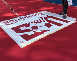
Vinyl Stencil
Precision-cut vinyl stencils for clean, easy application on walls, glass,...

Metal Cutting
High-precision metal cutting services delivering accurate, clean, and durable results...

FAA Airport Stencils
Durable, FAA-compliant stencils designed to create precise airfield pavement markings...

Acrylic Displays
Custom acrylic displays designed for clear, durable, and professional presentation...